2�
� RF Device Data�
� Freescale Semiconductor�
� MRF5S21130HR3 MRF5S21130HSR3�
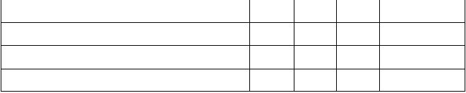
� Table 3. ESD Protection Characteristics�
� Test Conditions�
� Class�
� Human Body Model�
� 2 (Minimum)�
� Machine Model�
� M4 (Minimum)�
� Charge Device Model�
� C7 (Minimum)�
� Table 4. Electrical Characteristics (TC�
� = 25�
� °C unless otherwise noted)�
� Characteristic�
� Symbol�
� Min�
� Typ�
� Max�
� Unit�
� Off Characteristics�
� Zero Gate Voltage Drain Leakage Current�
� (VDS�
� = 65 Vdc, V�
� GS�
� = 0 Vdc)�
� IDSS�
� ?�
� ?�
� 10�
� μAdc�
� Zero Gate Voltage Drain Leakage Current�
� (VDS�
� = 28 Vdc, V�
� GS�
� = 0 Vdc)�
� IDSS�
� ?�
� ?�
� 1�
� μAdc�
� Gate-Source Leakage Current�
� (VGS�
� = 5 Vdc, V�
� DS�
� = 0 Vdc)�
� IGSS�
� ?�
� ?�
� 1�
� μAdc�
� On Characteristics�
� Gate Threshold Voltage�
� (VDS�
� = 10 Vdc, I�
� D�
� = 300 �
� μAdc)�
� VGS(th)�
� 2.5�
� 2.7�
� 3.5�
� Vdc�
� Gate Quiescent Voltage�
� (VDS�
� = 28 Vdc, I�
� D�
� = 1200 mAdc)�
� VGS(Q)�
� ?�
� 3.7�
� ?�
� Vdc�
� Drain-Source On-Voltage�
� (VGS�
� = 10 Vdc, I�
� D�
� = 3 Adc)�
� VDS(on)�
� ?�
� 0.26�
� 0.3�
� Vdc�
� Forward Transconductance�
� (VDS�
� = 10 Vdc, I�
� D�
� = 3 Adc)�
� gfs�
� ?�
� 7.5�
� ?�
� S�
� Dynamic Characteristics (1)�
� Reverse Transfer Capacitance �
� (VDS�
� = 28 Vdc �
� ±�
� 30 mV(rms)ac @ 1 MHz, V�
� GS�
� = 0 Vdc)�
� Crss�
� ?�
� 2.6�
� ?�
� pF�
� Functional Tests�
� (In Freescale Test Fixture, 50 ohm system) V�
� DD�
� = 28 Vdc, I�
� DQ�
� = 1200 mA, P�
� out�
� = 28 W Avg., f1 = 2112.5 MHz, �
� f2 = 2122.5 MHz and f1 = 2157.5 MHz, f2 = 2167.5 MHz, 2-carrier W-CDMA, 3.84 MHz Channel Bandwidth Carriers, ACPR measured in�
� 3.84 MHz Channel Bandwidth @ ±5 MHz Offset. IM3 measured in 3.84 MHz Channel Bandwidth @ ±10 MHz Offset. PAR = 8.5 dB @ 0.01%�
� Probability on CCDF.�
� Power Gain�
� Gps�
� 12�
� 13.5�
� ?�
� dB�
� Drain Efficiency�
� ηD�
� 24�
� 26�
� ?�
� %�
� Intermodulation Distortion�
� IM3�
� -37�
� -35�
� dBc�
� Adjacent Channel Power Ratio�
� ACPR�
� ?�
� -39�
� -37�
� dBc�
� Input Return Loss�
� IRL�
� ?�
� -12�
� -9�
� dB�
� 1. Part internally matched both on input and output.�
�  �
�
� � �  �
�
� � �  �
�
� � �  �
�
� � �  �
�
� � �  �
�
� � �  �
�
� � �  �
�
� � 发布紧急采购,3分钟左右您将得到回复。
相关PDF资料
MRF5S4125NR1
MOSFET RF SGL 450MHZ TO-270-4
MRF5S4140HSR5
MOSFET RF N-CHAN 28V 28W NI-780S
MRF5S9070MR1
MOSFET RF N-CH 26V 70W TO-270-2
MRF5S9070NR5
MOSFET RF N-CH 26V 70W TO-270-2
MRF5S9080NR1
MOSFET RF N-CH 26V 80W TO-270-4
MRF5S9100MR1
MOSFET RF N-CH 26V 20W TO-270-4
MRF5S9101MR1
MOSFET RF N-CH 26V 100W TO2704
MRF5S9150HSR5
MOSFET RF N-CHAN 28V 33W NI-780S
相关代理商/技术参数
MRF5S21130R3
制造商:MOTOROLA 制造商全称:Motorola, Inc 功能描述:The RF MOSFET Line RF Power Field Effect Transistor N-Channel Enhancement-Mode Lateral MOSFETs
MRF5S21130S
制造商:MOTOROLA 制造商全称:Motorola, Inc 功能描述:The RF MOSFET Line RF Power Field Effect Transistor N-Channel Enhancement-Mode Lateral MOSFETs
MRF5S21130SR3
制造商:MOTOROLA 制造商全称:Motorola, Inc 功能描述:The RF MOSFET Line RF Power Field Effect Transistor N-Channel Enhancement-Mode Lateral MOSFETs
MRF5S21150
制造商:FREESCALE 制造商全称:Freescale Semiconductor, Inc 功能描述:RF POWER FIELD EFFECT TRANSISTORS
MRF5S21150HR3
功能描述:MOSFET RF N-CHAN 28V 33W NI-880 RoHS:是 类别:分离式半导体产品 >> RF FET 系列:- 产品目录绘图:MOSFET SOT-23-3 Pkg 标准包装:3,000 系列:- 晶体管类型:N 通道 JFET 频率:- 增益:- 电压 - 测试:- 额定电流:30mA 噪音数据:- 电流 - 测试:- 功率 - 输出:- 电压 - 额定:25V 封装/外壳:TO-236-3,SC-59,SOT-23-3 供应商设备封装:SOT-23-3(TO-236) 包装:带卷 (TR) 产品目录页面:1558 (CN2011-ZH PDF) 其它名称:MMBFJ309LT1GOSMMBFJ309LT1GOS-NDMMBFJ309LT1GOSTR
MRF5S21150HR5
功能描述:MOSFET RF N-CHAN 28V 33W NI-880 RoHS:是 类别:分离式半导体产品 >> RF FET 系列:- 产品目录绘图:MOSFET SOT-23-3 Pkg 标准包装:3,000 系列:- 晶体管类型:N 通道 JFET 频率:- 增益:- 电压 - 测试:- 额定电流:30mA 噪音数据:- 电流 - 测试:- 功率 - 输出:- 电压 - 额定:25V 封装/外壳:TO-236-3,SC-59,SOT-23-3 供应商设备封装:SOT-23-3(TO-236) 包装:带卷 (TR) 产品目录页面:1558 (CN2011-ZH PDF) 其它名称:MMBFJ309LT1GOSMMBFJ309LT1GOS-NDMMBFJ309LT1GOSTR
MRF5S21150HSR3
功能描述:MOSFET RF N-CHAN 28V 33W NI-880S RoHS:是 类别:分离式半导体产品 >> RF FET 系列:- 产品目录绘图:MOSFET SOT-23-3 Pkg 标准包装:3,000 系列:- 晶体管类型:N 通道 JFET 频率:- 增益:- 电压 - 测试:- 额定电流:30mA 噪音数据:- 电流 - 测试:- 功率 - 输出:- 电压 - 额定:25V 封装/外壳:TO-236-3,SC-59,SOT-23-3 供应商设备封装:SOT-23-3(TO-236) 包装:带卷 (TR) 产品目录页面:1558 (CN2011-ZH PDF) 其它名称:MMBFJ309LT1GOSMMBFJ309LT1GOS-NDMMBFJ309LT1GOSTR
MRF5S21150HSR5
功能描述:MOSFET RF N-CHAN 28V 33W NI-880S RoHS:是 类别:分离式半导体产品 >> RF FET 系列:- 产品目录绘图:MOSFET SOT-23-3 Pkg 标准包装:3,000 系列:- 晶体管类型:N 通道 JFET 频率:- 增益:- 电压 - 测试:- 额定电流:30mA 噪音数据:- 电流 - 测试:- 功率 - 输出:- 电压 - 额定:25V 封装/外壳:TO-236-3,SC-59,SOT-23-3 供应商设备封装:SOT-23-3(TO-236) 包装:带卷 (TR) 产品目录页面:1558 (CN2011-ZH PDF) 其它名称:MMBFJ309LT1GOSMMBFJ309LT1GOS-NDMMBFJ309LT1GOSTR